
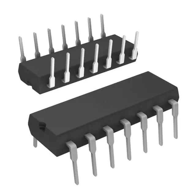
Abbildungen dienen nur als Referenz
CD4541BCN
+StücklisteIC OSC PROG TIMER 100KHZ 14DIP
-
HerstellerOnsemi
-
Herstellerteil #CD4541BCN
-
Datenblatt CD4541BCN DataSheet
-
Paket 14-DIP (0.300, 7.62mm)
-
Auf Lager4461
365 Tage Qualitätsgarantie
7*24 Stunden-Servicegarantie
90-Tage Kundendienstgarantie
Originalproduktgarantie
Spezifikationen
| Attribut | Wert |
| Supplier | onsemi |
| Package | Tube |
| ProductStatus | Obsolete |
| Type | Programmable Timer |
| Count | 65536 |
| Frequency | 100kHz |
| Voltage-Supply | 3V ~ 15V |
| OperatingTemperature | -55°C ~ 125°C |
| Package/Case | 14-DIP (0.300, 7.62mm) |
| SupplierDevicePackage | 14-MDIP |
Übersicht
Description
A key feature of the CD4541BCN is its ability to deliver precise time delays or pulse generation, which can be set through an external resistor and capacitor. The IC also offers a choice of four frequency divider options, which can be selected to adjust the timing intervals. With its built-in oscillator circuit, the CD4541BCN eliminates the need for external oscillators, simplifying circuit design.
The CD4541BCN is often used in applications including timing delays, clock generation, and pulse-width modulation. Its robust design makes it suitable for use in various environments, from industrial to consumer electronics.
Equivalent
Features
1. Programmable Timer: It can be configured for a wide range of timing intervals using external resistors and capacitors.
2. Modes of Operation: Offers both monostable (one-shot) and astable (free-running) modes, enabling flexibility in applications.
3. Oscillator Option: Provides an internal oscillator with an adjustable frequency for generating timing sequences.
4. Wide Supply Voltage Range: Operates over a broad voltage range from 3V to 15V, making it suitable for various power supply conditions.
5. Low Power Consumption: Features low power dissipation, ideal for battery-operated devices.
6. High Noise Immunity: CMOS technology ensures high noise margin and robustness against interference.
7. Temperature Range: Typically operates over a standard temperature range, making it reliable in different environmental conditions.
8. Output Options: Supports buffered and unbuffered output options for different driving requirements.
9. Reset Functionality: Includes a master reset pin to facilitate easy resetting of the timer.
These features make the CD4541BCN suitable for timing, delay, and oscillator applications in consumer electronics, industrial controls, and other applications.
Pinout
1. VDD (Pin 14): Supply voltage.
2. VSS (Pin 7): Ground.
3. Q/Q̅ (Pin 8/Pin 9): Outputs; Q is the normal output, and Q̅ is the inverted output.
4. RESET (Pin 6): Resets the timer.
5. MR (Master Reset) (Pin 5): Resets and initializes the device.
6. A and B (Pin 12 and Pin 11): Timer control pins for setting the mode of operation.
7. CAP (Pin 3): Timing capacitor connection.
8. RC (Pin 2): Connection for the resistor-capacitor timing network.
9. AUTO/MAN (Pin 1): Selects automatic or manual reset mode.
10. EN (Pin 13): Enables the oscillator.
11. NC (Pins 4 and 10): No internal connection.
The CD4541BCN can be configured for various timing applications using these pins, allowing for flexible operation in timing and oscillator circuits.




