
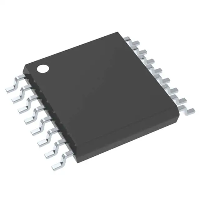
Abbildungen dienen nur als Referenz
SN74CB3Q3257PW
+StücklisteIC MUX/DEMUX 4 X 2:1 16TSSOP
-
HerstellerTexas Instruments
-
Herstellerteil #SN74CB3Q3257PW
-
Paket TSSOP-16
-
Auf Lager1867
365 Tage Qualitätsgarantie
7*24 Stunden-Servicegarantie
90-Tage Kundendienstgarantie
Originalproduktgarantie
Spezifikationen
| Attribut | Wert |
| Package / Case | Bulk,Tube |
| Series | 74CB |
| Part Status | Active |
| Type | Multiplexer/Demultiplexer |
| Circuit | 4 x 2:1 |
| Independent Circuits | 1 |
| Voltage Supply Source | Single Supply |
| Voltage - Supply | 2.3V ~ 3.6V |
| Operating Temperature | -40°C ~ 85°C |
| Mounting Type | Surface Mount |
Übersicht
Description
Key features of the SN74CB3Q3257PW include its ability to operate in a voltage range of 2.3 V to 3.6 V, and it supports rail-to-rail switching, ensuring compatibility with a wide array of digital signals. The device offers a low propagation delay and is designed with a breakout circuitry that allows for hot insertion capability, enhancing its robustness in dynamic environments.
The PW suffix denotes the TSSOP (Thin Shrink Small Outline Package) version, which is compact and suitable for space-constrained applications. Typical use cases include signal routing, data multiplexing, and bus isolation in communication, computing, and consumer electronics.
Equivalent
1. ON Semiconductor's MC74VCX3257
2. NXP's 74LVC1G57
3. Fairchild's FST3257
4. Diodes Incorporated's PI3LVD412
Each of these offers similar functionality with variations in features such as voltage levels, propagation delay, and power consumption. Always check the datasheets for compatibility with your specific application requirements.
Features
1. High-Speed Performance: Offers low ON-state resistance for high-speed data transmission.
2. Voltage Range: Operates over a wide voltage range from 2.3 V to 3.6 V.
3. I/O Ports: Configurable as four 1-of-2 multiplexer/demultiplexer.
4. Low Power Consumption: Features low power dissipation with a low-power mode.
5. Signal Integrity: Provides excellent signal integrity with low crosstalk.
6. Bandwidth: Supports high bandwidth, making it suitable for high-speed applications.
7. Control Inputs: Uses standard logic levels for control inputs.
8. Compact Package: Available in TSSOP package for space-constrained applications.
9. Enhanced ESD Protection: Includes protection against electrostatic discharge.
This device is suitable for a range of applications requiring signal routing and multiplexing, such as in communication systems and digital signal processing.
Pinout
- Pins 1, 7, 10, and 15 are the source inputs for the multiplexers.
- Pins 2, 5, 11, and 14 are the drain outputs.
- Pin 3 is the switch enable input (OE\), which is active low.
- Pin 13 is the select input (S), which determines which channel is connected to the drain.
- Pin 4 is VCC, which is the power supply pin.
- Pin 12 is GND, which is the ground connection.
This device allows for efficient signal routing in circuits through its low ON-state resistance, making it suitable for both digital and analog applications. It operates in a wide supply voltage range and has features that minimize the risk of signal degradation.





